
A new report coming from South Korea suggests Samsung Foundry has reached an important milestone in its 4nm FinFET process production. According to SEDaily, Samsung Foundry has surpassed the 80% yield rate for its 4nm process, which means it is now firmly in the process maturity stage.
Samsung Foundry process technology roadmap
This development positions Samsung to go head-on with rival TSMC in meeting all-time high memory chip demand from big tech firms. Samsung Electronics’ Pyeongtaek Campus, which also produces 5nm and 7nm chips, is now ready to supply its 4nm chips to AI accelerators as well as clients in the automotive and mobile tech spheres. Samsung Foundry’s 4nm process is also notably used as the base die for the sixth-generation HBM4 memory chips.
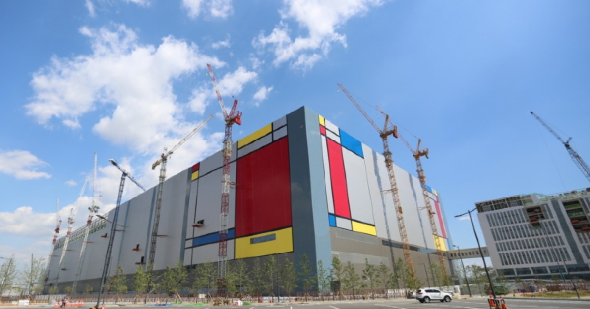
Samsung Electronics’ Pyeongtaek Campus
With six years of mass producing 4nm chips under its belt, Samsung’s now mature 4nm process is set to help the company limit the blows of rising memory prices and return to profitability in the second half of this year.
Source (in Korean)


